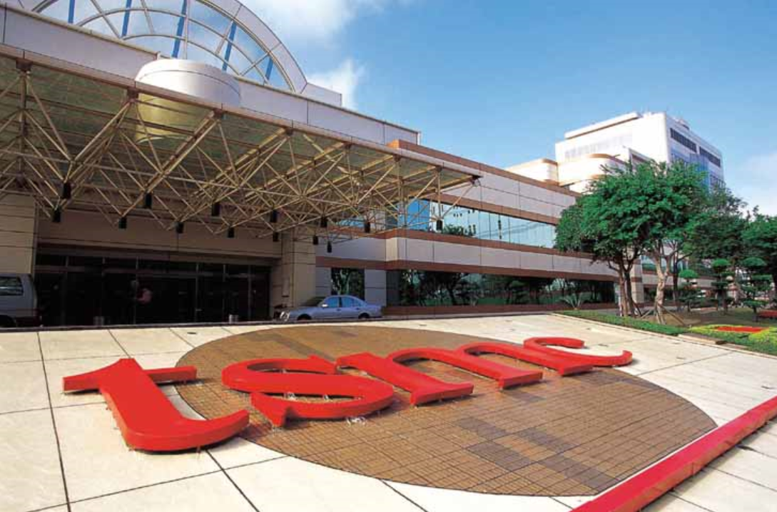
The world’s largest contract foundry is Taiwan Semiconductor Manufacturing Company (TSMC). The company makes chips for companies that design theirs but don’t have the facilities to produce them. The equipment used to make chips is very complex and very expensive. For example, TSMC plans to spend $ 15 billion this year on capital expenditures. TSMC’s main clients include Apple, Qualcomm and Huawei.
TSMC to start risk production of 3nm process node next year
This year, both Apple and Huawei will receive their most advanced chipsets, the A14 Bionic and HiSilicon Kirin 1020, respectively. Both will be done using TSMC’s 5nm process node, meaning the number of transistors within components will increase by approximately 77%. This makes the chips more powerful and energy efficient than the 7nm chips they replace. Due to new US export rules, TSMC will not be able to ship components to Huawei from the second half of September. The United States is preventing any foundry that uses American technology to send semiconductors to Huawei without obtaining a license. The foundry said the other day that it will not send wafers to Huawei after September 14. TSMC CEO Mark Liu has yet to comment on whether he will attempt to obtain a US license that allows him to continue doing business with the Chinese manufacturer.
TSMC’s 5nm process node is being used to manufacture the Bionic A14 chip that will power the iPhone 12 series
As a general rule, the more transistors there are on a chip, the more powerful and efficient the energy is. About every two years, the density of the transistor almost doubles, allowing companies to design more powerful components. As an example, there will be 15 billion transistors inside the Apple A14 Bionic compared to the 8.5 billion packaged inside the A13 Bionic and the 6.9 billion that were shod in the A12 Bionic. If things go as planned, the Apple iPhone 12 series will be the first phone to be powered by a 5nm chipset.
The first 5nm Snapdragon chip to be shipped by TSMC was expected to be the Snapdragon 875 mobile platform. This chipset will power most Android flagships from the first half of 2021 and will include ARM’s new Super-core Cortex X1. The latter could improve the performance of chips using ARM’s Cortex-A77 core by 30%. However, a recent report suggests that TSMC’s main rival, Samsung Foundry will produce the Snapdragon 875G using its 5nm EUV process. EUV, or extreme ultraviolet lithography, uses extremely thin ultraviolet light to etch patterns into dies to show where transistors are supposed to be placed.
TSMC has said it will build a factory in the US That will start production in 2023. However, it will reportedly produce 5nm chips when it goes online, which will be a generation behind the 3nm components. that will come out of TSMC’s assembly lines at its factories in Asia.
And now TSMC is looking towards 3nm mode. According to MyDrivers, the smelter plans to start risk production at the 3nm process node next year. As we pointed out in April, these are chips produced by the foundry for manufacturers willing to buy them without going through standard testing procedures. TSMC says its 3nm chips will offer a 10% to 15% increase in performance with a 20% to 25% increase in energy efficiency. Today’s report mentions that Apple’s A16 chip, which will ship in 2022, will be manufactured using the 3nm process node.
TSMC originally planned to make a change from using FinFET transistors to GAA (gate-all-around) for the 3nm process node. But the foundry has decided to continue using FinFET to control the current going through the transistors until it is ready to move towards the 2nm node.