
Credit: Samuel Howell / 2020 EPFL
EPFL researchers have developed high-precision technology that enables them to carve nanometric patterns into two-dimensional materials.
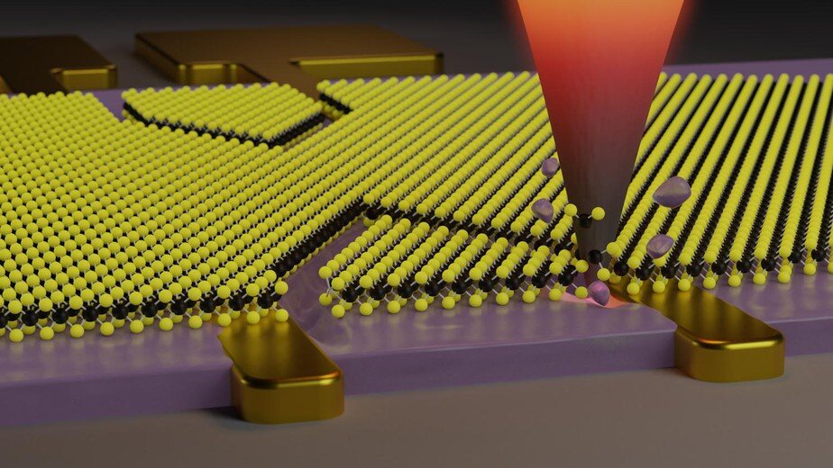
With its pioneering nanotechnology, EPFL researchers have accomplished the impossible. They can now use heat to break the bonds between atoms with a miniature scalpel. “It is extremely difficult to structure two-dimensional materials using conventional lithography, which often employs aggressive chemicals or electrically charged accelerated particles, such as electrons or ions, that can damage the properties of the material,” says Xia Liu, a researcher and postdoctoral fellow at the school. of the Microsystems Engineering Laboratory. “However, our technique uses a localized ‘source’ of heat and pressure to precisely cut two-dimensional materials.”
“Our technology is similar to the art of paper cutting, which is common in this region of Switzerland, but on a much smaller scale,” explains Ana Conde Rubio, co-author of the study. “We use heat to modify the substrate to make it more flexible, and in some cases even convert it to a gas. Then we can more easily carve into the 2-D material.”
A sharp point
Xia Liu, Samuel Howell, Ana Conde Rubio, Giovanni Boero and Jürgen Brugger used molybdenum ditelluride (MoTetwo), a two-dimensional material that is similar to graphene. It is less than a nanometer, or three layers of atoms, thick. The MoTetwo It is placed on a polymer that reacts to changes in temperature. “When the polymer is exposed to heat, it sublimes, which means it goes from a solid state to a gaseous state,” explains Liu.
Researchers at the Institute for Microengineering used a new nanoscale structuring technique called thermal exploration probe lithography (t-SPL), which works similarly to an atomic force microscope. They heat a nanosized sharp tip to over 180 ° C, bring it into contact with the 2-D material and apply a little force. This causes the polymer to sublimate. A thin layer of MoTe2 comes off without damaging the rest of the material.
Small and more efficient components.
Researchers will be able to use this technology to carve extremely precise patterns into 2-D materials. “We use a computer-driven system to monitor the ultrafast heating and cooling process and the position of the tip,” explains Samuel Howell, another co-author. “This allows us to make predefined indents to create, for example, the nanoribons used in nanoelectronic devices.”
But what’s the use of working on such a small scale? “Many two-dimensional materials are semiconductors and can be integrated into electronic devices,” says Liu. “This generic technology will be very useful in nanoelectronics, nanophotonics, and nanobiotechnology, as it will help make electronic components smaller and more efficient.”
Improving precision
The next phase of the research will focus on looking at a wider range of materials and finding combinations that work in integrated nanosystems. Future activities will also review the cantilever design and nanotip to improve nanocut performance.
More generally, scientists at the Microsystem Laboratory are seeking to develop a new generation of manufacturing techniques for flexible microsystems. “Polymer-based microelectromechanical systems (MEMS) have many potential electronic and biomedical applications,” explains Professor Jürgen Brugger. “But we are still in the early stages of developing techniques to design functional polymers in 3-D microsystems.” Brugger hopes to push the boundaries and find new materials and processes for MEMS by focusing on stenciling, the printing process, targeted nanomaterial self-assembly, and localized thermal processing.
Two-dimensional materials lose heat more easily when enclosed
Xia Liu et al. Thermomechanical nanocutting of 2D materials, Advanced materials (2020). DOI: 10.1002 / adma.202001232
Provided by Ecole Polytechnique Federale de Lausanne
Citation: Researchers cut nanometer-size patterns in two-dimensional materials (2020, June 23) retrieved June 24, 2020 from https://phys.org/news/2020-06-nanometer-sized-patterns-d-materials .html
This document is subject to copyright. Other than fair dealing for private research or study purposes, no part may be reproduced without written permission. The content is provided for informational purposes only.
