[ad_1]
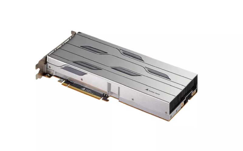
Shanghai Tianshu Intellectual Semiconductor Co. (Tianshu Zhixin) announced earlier this week that it was close to bringing its first homegrown 7nm General Purpose GPU (GPGPU), Big Island (BI), to mass production and commercial delivery.
COMMERCIAL
Tianshu Zhixin comes months after Big Island was first announced earlier in the year. Back then, the Chinese chipmaker hinted that BI was being made with a 7nm process node, along with a 2.5D chip on water on substrate (CoWoS). The company did not mention which 7nm process it was using for its GPGPU, but Tom’s Hardware has confirmed that it is a 7nm from TSMC foundries.
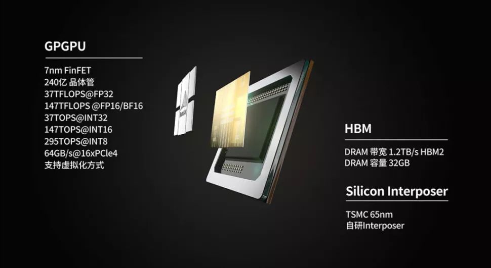
In addition to his “mass production” announcement, Tianshan Zhixin also shared information about BI in the form of a slide. It is written in Chinese, but from what we can tell, the GPGPU uses a 32GB HBM2 memory with speeds up to 1.2TB / s. There’s also a long list of its performance in floating point operations, including the usual FP32 and FP16 performance metrics.
At the time of writing, Tianshu Zhixin did not say when his first round of BI GPGPU is scheduled to ship, nor did he say who his first group of clients would be.
(Source: Tom’s Hardware)
[ad_2]
