, a two-dimensional semiconductor. The only layer of WSe2 is sitting on a layer of boron nitride (blue and gray balls). Credit: Nicholas Borys / Montana State University")
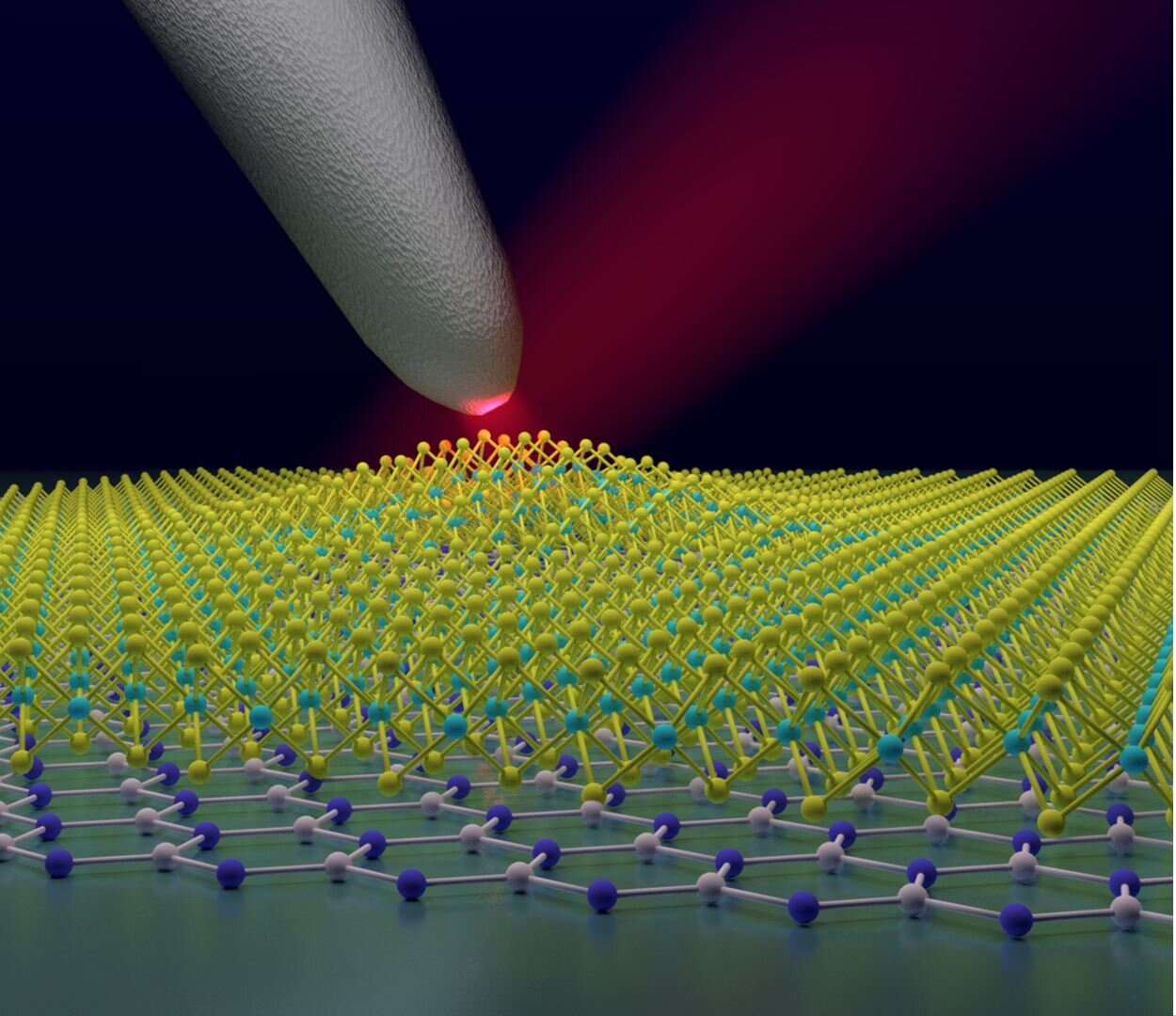
Schematic of a laser-illuminated nano-optical probe investigating a tungsten dyselenide-tensioned nanobubble (WSe2; green and yellow balls), a two-dimensional semiconductor. The only layer of WSe2 is sitting on a layer of boron nitride (blue and gray balls). Credit: Nicholas Borys / Montana State University
July 13, 2020 – Columbia Engineering and Montana State University researchers reported today that they discovered that putting enough stress on a 2-D material (tungsten dyselenide (WSe2)) creates localized states that can produce single-photon emitters. . Using sophisticated light microscopy techniques developed at Columbia over the past three years, the team was able to obtain direct images of these states for the first time, revealing that even at room temperature they are highly adjustable and act as quantum dots, tightly confined semiconductor pieces to emit light
“Our discovery is very exciting, because it means that we can now place a single-photon emitter wherever we want and adjust its properties, such as the color of the emitted photon, by simply bending or stretching the material at a specific location.” says James Schuck, an associate professor of mechanical engineering, who co-led the study published today by Nanotechnology nature. “Knowing exactly where and how to tune into the single-photon emitter is essential to creating quantum optical circuits for use in quantum computers, or even in so-called ‘quantum’ simulators that mimic physical phenomena too complex to model with today’s computers.”
The development of quantum technologies such as quantum computers and quantum sensors is a rapidly developing field of research as researchers discover how to use the unique properties of quantum physics to create devices that can be much more efficient, faster, and more sensitive than existing technologies. For example, quantum information (think of encrypted messages) would be much more secure.
Light is made up of discrete packets of energy known as photons, and light-based quantum technologies are based on creating and manipulating individual photons. “For example, a typical green laser pointer emits more than 1016 (10 trillion) photons every second at the push of a button,” says Nicholas Borys, an assistant professor of physics at Montana State University and co-PI of this new study. . “But developing devices that can produce a single controllable photon at the flip of a switch is extremely difficult.”
Researchers have known for five years that single-photon emitters exist in ultrathin 2D materials. Their discovery was greeted with great excitement that single-photon emitters in 2-D materials can be more easily tuned and integrated more easily into devices than most other single-photon emitters. But no one understood the underlying properties of the material that lead to the emission of a single photon in these two-dimensional materials. “We knew that single-photon emitters existed, but we didn’t know why,” says Schuck.
In 2019, an article came out from the group of Frank Jahnke, a professor at the Institute of Theoretical Physics at the University of Bremen, Germany, who theorized how tension in a bubble can cause wrinkles and localized states for the emission of a single photon. Focusing on detection and engineering phenomena emerging from nanostructures and interfaces, Schuck was immediately interested in collaborating with Jahnke. He and Borys wanted to focus on the tiny nanoscale wrinkles that form in the form of donuts around the bubbles that exist in these ultrathin 2D layers. Bubbles, typically small pockets of fluid or gas that become trapped between two layers of two-dimensional materials, create tension in the material and lead to the formation of wrinkles.
 and a layer of hexagonal boron nitride (hBN), an insulating material. On the left, the WSe2 layer has folded over on itself, forming a bilayer (2L-WSe2), which contains additional bubbles and wrinkles. Credit: Thomas Darlington / Columbia Engineering")
An atomic force microscope image showing nanobubbles formed between a single layer of the two-dimensional semiconductor WSe2 (1L-WSe2) and a layer of hexagonal boron nitride (hBN), an insulating material. On the left, the WSe2 layer has folded over on itself, forming a bilayer (2L-WSe2), which contains additional bubbles and wrinkles. Credit: Thomas Darlington / Columbia Engineering
Schuck’s group, and the field of two-dimensional materials, faced a major challenge in studying the origins of these single-photon emitters: the tense nanoscale regions, which emit the light of interest, are much smaller, approximately 50,000 times smaller. smaller than the thickness of a human hair, which can be solved with any conventional light microscope.
“This makes it difficult to understand what specifically in the material results in the emission of a single photon: is it just the high voltage? Is it due to hidden defects within the filtered region?” says the study’s lead author, Tom Darlington, who is a postdoctoral fellow and a former Schuck graduate researcher. “Light is needed to observe these states, but their sizes are so small that they cannot be studied with standard microscopes.”
Working with other laboratories at the Columbia Nano Institute, the team leveraged their decades of experience in nanoscale research. They used sophisticated light microscopy techniques, including their new microscopy capabilities, to observe not only nanobubbles, but even within them. Their advanced “nano-optical” microscopy techniques, their “nanoscopes,” allowed them to image these materials at a resolution of ~ 10nm, compared to the resolution of about 500nm that can be achieved with a conventional light microscope.
Defects are thought by many researchers to be the source of single-photon emitters in two-dimensional materials, as they are generally found in three-dimensional materials such as diamond. To rule out the role of defects and demonstrate that the strain alone could be responsible for the individual photon emitters in 2-D materials, Schuck’s group studied the ultra-low defect materials developed by Jim Hone’s group at Columbia Engineering, part of the materials financed by NSF Center for Research in Science and Engineering. They also took advantage of new double-layered structures developed within the Center for Programmable Quantum Materials (a DOE Energy Frontier Research Center), which provided well-defined bubbles on a platform that was easily studied with Schuck’s optical “nanoscopes”.
“Atomic-scale defects are often attributed to localized sources of light emission in these materials,” says Jeffrey Neaton, professor of physics at UC Berkeley and Director of the Associated Laboratory for Energy Sciences, Lawrence Berkeley National Laboratory, who did not participated in the study. . “The emphasis in this work on the fact that stress alone, without the need for defects at the atomic scale, can potentially impact[s] applications ranging from low power light emitting diodes to quantum computers. “
Schuck, Borys and their teams are now exploring how voltage can be used to precisely tailor the specific properties of these single-photon emitters and to develop pathways to engineering adjustable and addressable arrays of these emitters for future quantum technologies.
“Our results mean that fully adjustable room temperature single photon emitters are now within our grasp, paving the way for practical and controllable quantum photonic devices,” observes Schuck. “These devices can be the foundation of quantum technologies that will profoundly change information, detection and information technology as we know it.”
Scientists create new device to light the way for quantum technologies
Images of excitons located in WSe2 monolayer nanoscale bubble strains at room temperature, Nanotechnology nature (2020). DOI: 10.1038 / s41565-020-0730-5
Provided by Columbia University College of Engineering and Applied Sciences
Citation: Little bubbles make a quantum leap (2020, July 13) retrieved on July 13, 2020 from https://phys.org/news/2020-07-tiny-quantum.html
This document is subject to copyright. Other than fair dealing for private study or research purposes, no part may be reproduced without written permission. The content is provided for informational purposes only.
