After yesterday’s preview, Qualcomm fully unveiled its new Snapdragon 888 chipset today. It’s a 5nm chip with next-generation architecture. The first devices with the 888 will come out in the first quarter of next year, several smartphone manufacturers are already competing for who will be the first.
There’s a lot to cover so settle in.
CPU
The 888 is the first chip to go official with the Cortex-X1 core (ARM’s base design has some Qualcomm tweaks). Compared to the A78, the X1 can execute 33% more instructions per clock, has twice the hardware SIMD, and the capacity of the L1 and L2 caches has also doubled. This core runs at 2.84 GHz.
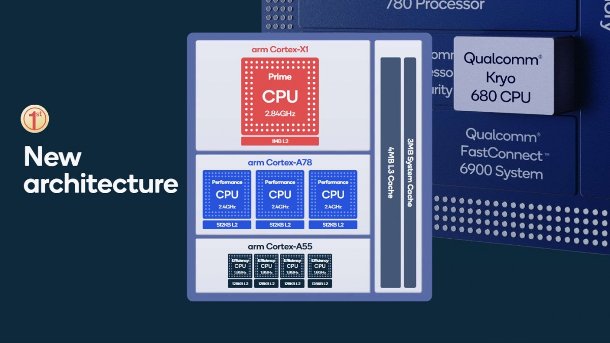
Next is a group of three Cortex-A78 cores clocked at 2.4 GHz. They are joined by four A55 cores operating at 1.8GHz. The CPU is also equipped with 4 MB of L3 cache and 3 MB of system cache.
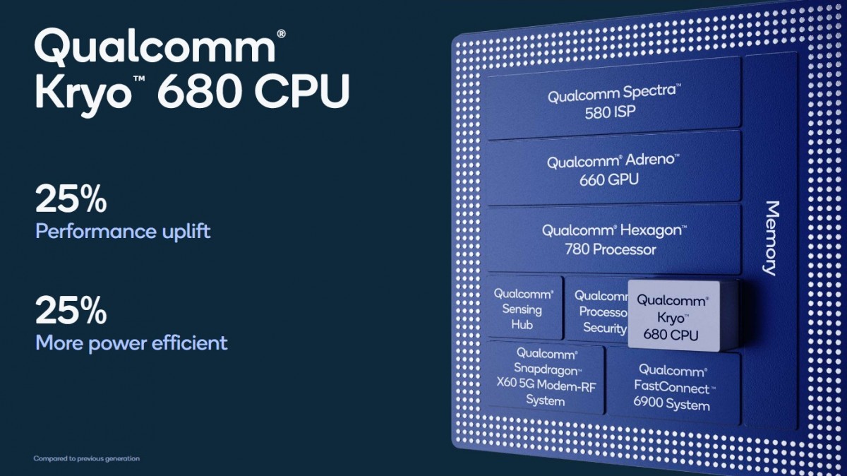
In total, the Kryo 680 CPU promises a 25% performance increase over the S865 chipset processor. Energy efficiency also increased by 25%.
GPU
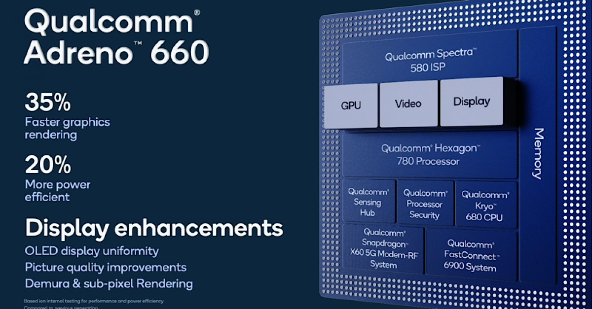
The Adreno 660 aims for 35% faster rendering performance while increasing energy efficiency by 20%. It is designed for games with high frame rates and low latency. The goal is to allow 144fps playback for games that want it, but there are also various features to improve image quality.
Variable Speed Shader (VRS) is a new trick found on recent GPUs from Nvidia and AMD (including those on the PS5 and Xbox consoles). Allow shaders to work on two or four pixels at a time, instead of just one.
This saves computational resources, and if game developers are careful how they apply it, the rendered frame will be visually indistinguishable. VRS can increase performance by up to 30%. Alternatively, it can be used to increase energy efficiency.
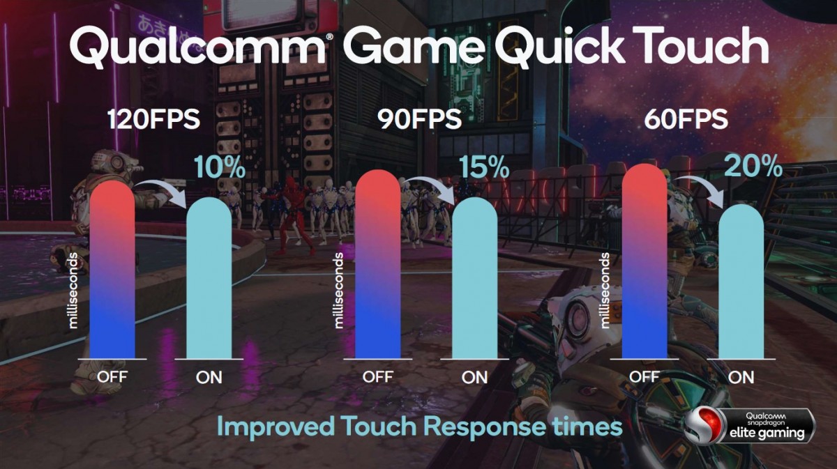
Game Quick Touch can reduce touch latency by up to 20%. This works at up to 120fps, but is most effective at 60fps, so all games can use it, even if they don’t support higher frame rates.
The Adreno 660 supports 10-bit HDR and sub-pixel rendering. It can also improve the uniformity of OLED displays with Mura compensation (“mura” or “cloudiness” is the result of uneven calibration of neighboring pixels).
Camera
The 888 is the first Snapdragon with a triple ISP (previous 800 series chips had dual ISPs). This allows three separate camera sequences to be processed simultaneously, which has multiple uses. For one, it can handle three 4K HDR video streams or capture three 28MP photos at the same time.
This will also make transitions smooth from ultrawide to wide cameras to tele, as each camera has its own ISP. Previous three camera / two ISP designs resulted in a “jump” when the phone switched between video transmissions.
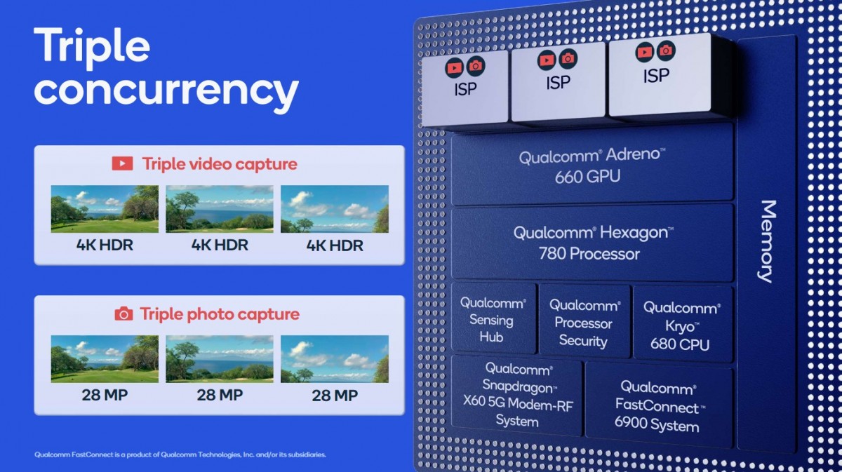
All three Spectra 580 ISPs are also used for tiered HDR, as they can process short, medium and long exposures simultaneously. The S888 can record 10-bit HDR photos in the HEIF image format, in addition to the HDR video capabilities of its predecessor (the S865 introduced HDR10 + and Dolby Vision support for video).
Speaking of videos, the new chipset can capture and play 4K video at 120fps, so you can take full advantage of a high-resolution 4K display. Returning to photography, the chip can take 120 photos per second with a resolution of 12MP.
Connectivity
This is the first chipset to use the Snapdragon X60 5G modem. And unlike the 865, the modem is built-in rather than an external chip. This 3rd generation modem supports 5G sub-6 and mmWave flavors. It offers downlink speeds of up to 7.5 Gbps and uplinks of up to 3 Gbps.
The FastConnect 6900 system features 6G Wi-Fi (axis in the 6 GHz band) and can reach speeds of up to 3.6 Gbps, the fastest mobile Wi-Fi in the industry, says Qualcomm. The 6E standard also offers lower latency, an advantage for streaming games from a local PC (or the cloud, there the 5G modem can help too).
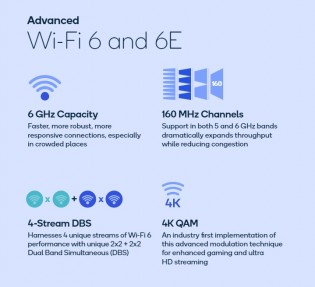
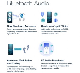
FastConnect 6900 supports Wi-Fi 6E and advanced Bluetooth 5.2 technology
Bluetooth 5.2 with dual antennas is also supported, in addition to the aptX suite of high-quality, low-latency wireless audio technology.
AI
The sixth-generation AI engine combines the new Hexagon 780 and the number processing power of the GPU to deliver 26 TOPS (compared to 15 TOPS in the S865). Energy efficiency has also improved enormously, performance per watt has increased up to 3 times.
The second generation Sensing Hub also reduces energy use. It can operate at less than 1 milliamp, but it can handle much more than the 1st gen – now 80% of simple AI tasks go through the Hub instead of having to activate the powerful Hexagon processor. This is for simple applications like activity and elevation detection and listening to wake words.
Security
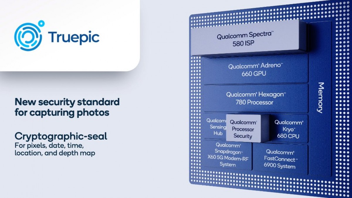
The Snapdragon 888 is the first mobile chipset to comply with the Content Authenticity Initiative standard. You can capture cryptographically sealed photos, which include tamper-resistant metadata that proves an image is authentic (but does so in a privacy-sensitive way).
The 888 also features a hypervisor, a feature that was first added to the PC-oriented 8cx Gen 2 chip. This is more of a server and desktop feature as it allows multiple operating systems to run on the same hardware while being completely separated from each other (so if one is compromised, the security of the others is not affected) .
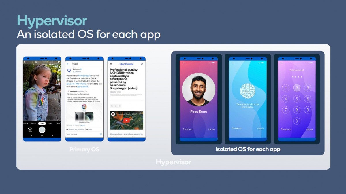
Each application can be run on its own operating system instance for maximum security. It’s unclear if we’ll see this on Android, but it’s clear that the Snapdragon 888 will be used on ARM-powered tablets and computers as well, where such virtualization is much more common.
Loading
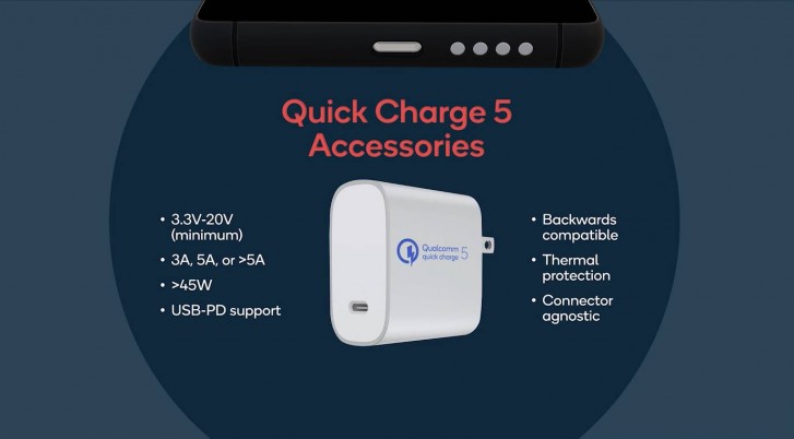
This wasn’t featured much today as QuickCharge 5 was announced months ago. The new Snapdragon supports this, of course, which means that it can handle a fast charge of more than 100W while keeping the heat to a minimum. It is compatible with USB Power Delivery and backwards compatible with previous QC generations dating back to 2.0.
The Snapdragon 888 will be used in devices coming early 2021. Xiaomi called dibs, Motrola will use it in an affordable Moto G phone, many other manufacturers have also announced plans for phones with 888 technology.